
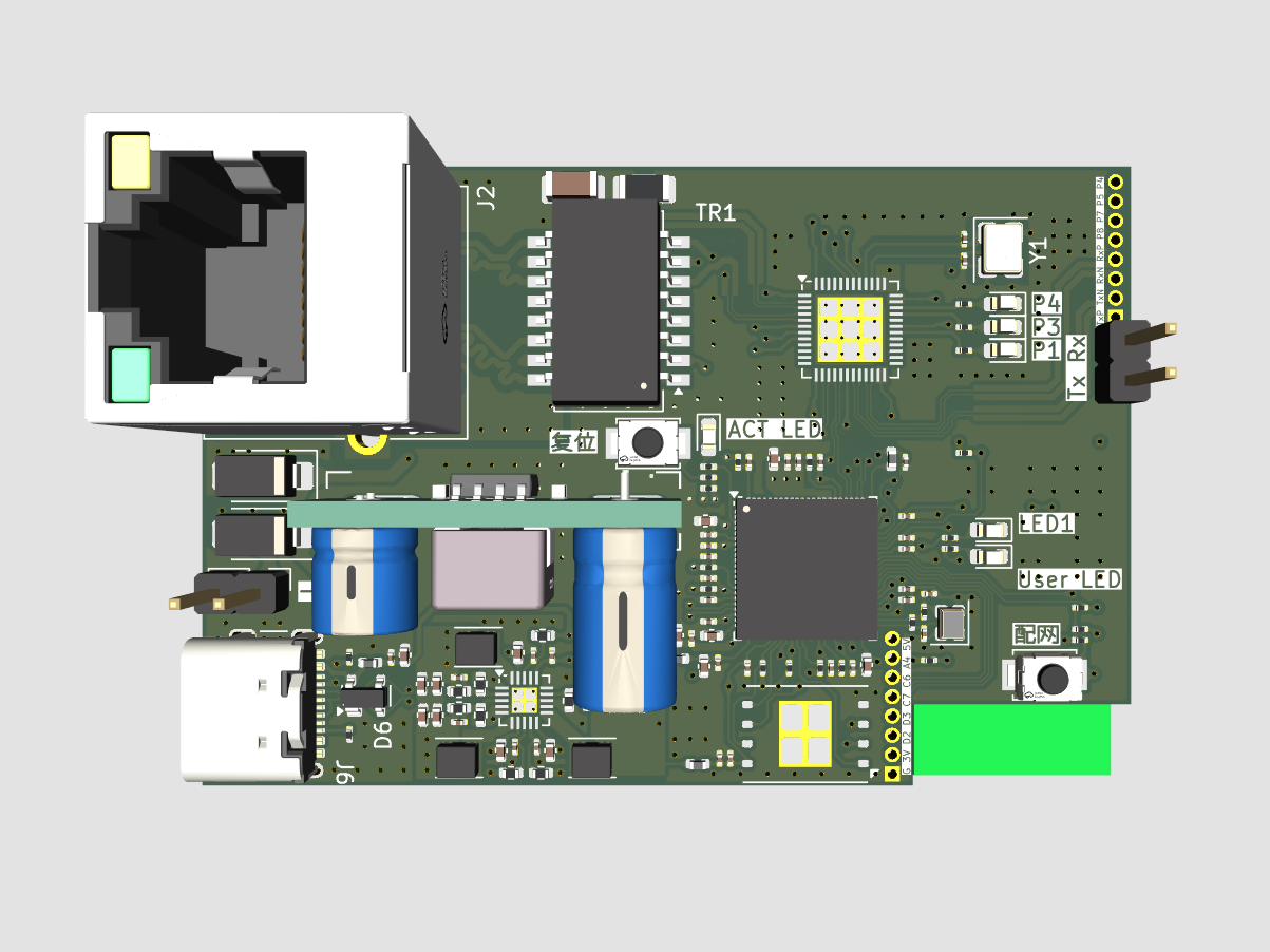
4-Layer High-Density Mainboard PCB Layout
Background
A smart hardware customer commissioned the PCB layout of a 4-layer high-density mainboard. The customer supplied the schematic and mechanical requirements; we handled placement and routing, stack-up design, impedance control and production file output. The board integrates an RV1103 main controller, a five-port Ethernet switch (RTL8305NB) with magnetics transformer, SPI NAND storage, multiple power rails and a third-party wireless module — high functional density in a very limited routing area.
Design Constraints
- Extremely tight space: the board outline is only 60×40 mm, the main controller is a QFN-88 package with 0.35 mm pitch, and the board uses a high proportion of 0201 components;
- Multiple power domains: close to ten supply rails from the 24 V input down to the core voltage require careful partitioning and decoupling;
- Impedance control: Ethernet and USB differential pairs need controlled impedance, and the Ethernet path passes through a magnetics transformer, so reference planes cannot be interrupted;
- Interface and module zoning: the board integrates an Ethernet port and a third-party wireless module, so interface, RF and power areas must be planned up front;
- EMC and protection: common-mode chokes, ESD arrays and input protection devices mean placement and routing directly affect results;
- Manufacturability: 0201 components demand careful pad design and DFM rules.
Design Highlights
Stack-up and impedance design
A 4-layer stack-up defines the relationship between signal layers and reference planes, with Ethernet differential pairs controlled to 100 Ω and USB pairs to 90 Ω.
0.35 mm pitch QFN fan-out
Routing between pads combined with nearby vias into inner layers completes the fan-out, with power and ground pins escaped first to keep the inner planes intact.
Power and plane planning
The board is partitioned by power domain with decoupling placed close to each rail, and dedicated planes for the core and DDR supplies reduce cross-coupling.
Differential pairs and isolation
Ethernet differential pairs are length-matched with a continuous reference plane, and the transformer provides isolation with no routing across plane splits.
Crystals and sensitive circuits
The two crystals (25 MHz and 24 MHz) sit close to their respective devices with ground guarding, kept away from parallel high-speed routing.
EMC and DFM
Protection devices sit close to the interfaces with short return paths; trace widths, clearances and vias follow the PCB house's process capability, and panelisation and process edges are included.
Delivery and Verification
- Deliverables: Gerber, stencil, assembly drawing, impedance report, pick-and-place data, panelisation drawing;
- Prototyping passed on the first run, with no re-spin caused by layout issues.
Application Value
- High-density routing and multi-rail power planning were completed within a 4-layer, 60×40 mm board, keeping layer count and cost under control;
- Controlled differential impedance and proper isolation lay the groundwork for reliable Ethernet and USB communication;
- First-pass prototyping saved the customer a full re-spin cycle;
- Manufacturing files follow the PCB house's process capability, reducing back-and-forth;
- A complete production package allows the project to move straight into volume preparation.