
Schematic
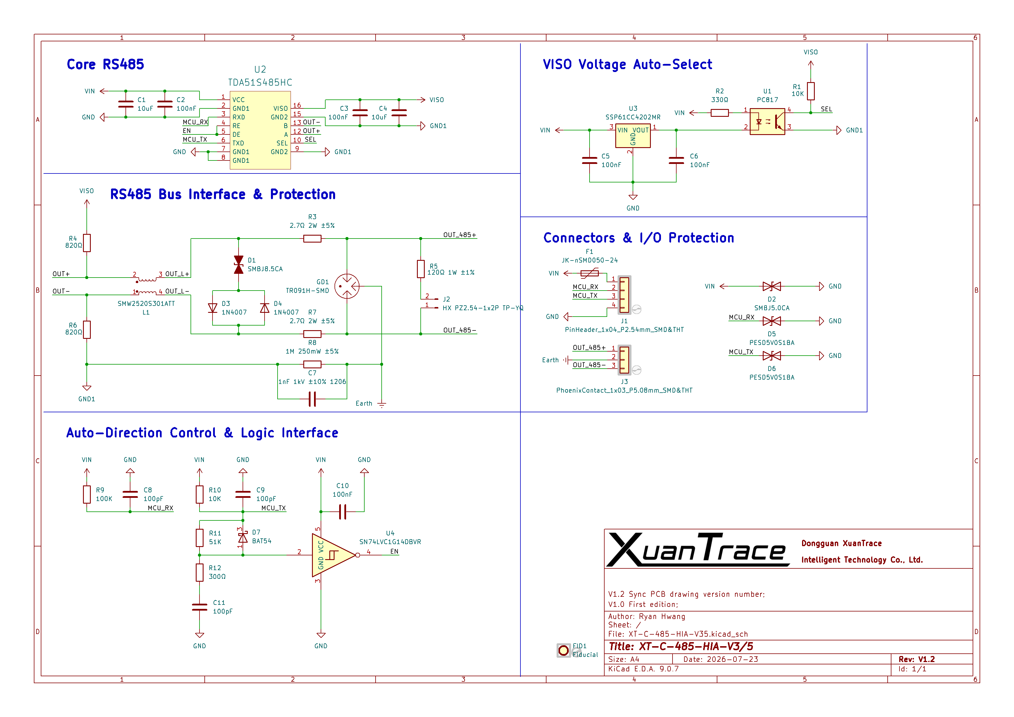
Full-board schematic, Rev V1.2. Click to enlarge.
Blocks
| Block | Contents |
|---|---|
| Core RS485 | Isolated transceiver U2, with decoupling on both sides |
| VISO Voltage Auto-Select | Isolated-side supply auto-sensing, which decides whether the isolated-side output level follows a 3.3 V or 5 V system |
| RS485 Bus Interface & Protection | Bus protection chain: current-limiting resistors → TVS → gas discharge tube → common-mode choke; includes the 120 Ω termination and the fail-safe bias |
| Connectors & I/O Protection | Logic-side J1 header and bus-side J3 terminal, plus the input resettable fuse and ESD diodes |
| Auto-Direction Control & Logic Interface | Schmitt-trigger shaping and automatic RE / DE direction switching |
Cross-checks
- Logic-side
J1: 2.54 mm header,VIN/RX/TX/GND - Bus-side
J3: 5.08 mm terminal, netsOUT_485+/Earth/OUT_485-(pin order is in the Pinout) PE(Earth) is separate from the logic-sideGND/GND1:PEis only for discharge and shielding; the two do not share groundJ1/J3use SMD & THT pads: one board can be either surface-mounted or through-hole mounted- The 120 Ω termination is provided by
R5, connected or disconnected with theJ2jumper
Full parameters are in Specifications; the summary table is on the product page.