
Pinout
The silkscreen reads top to bottom, viewed from above.
Logic Side (2.54 mm)
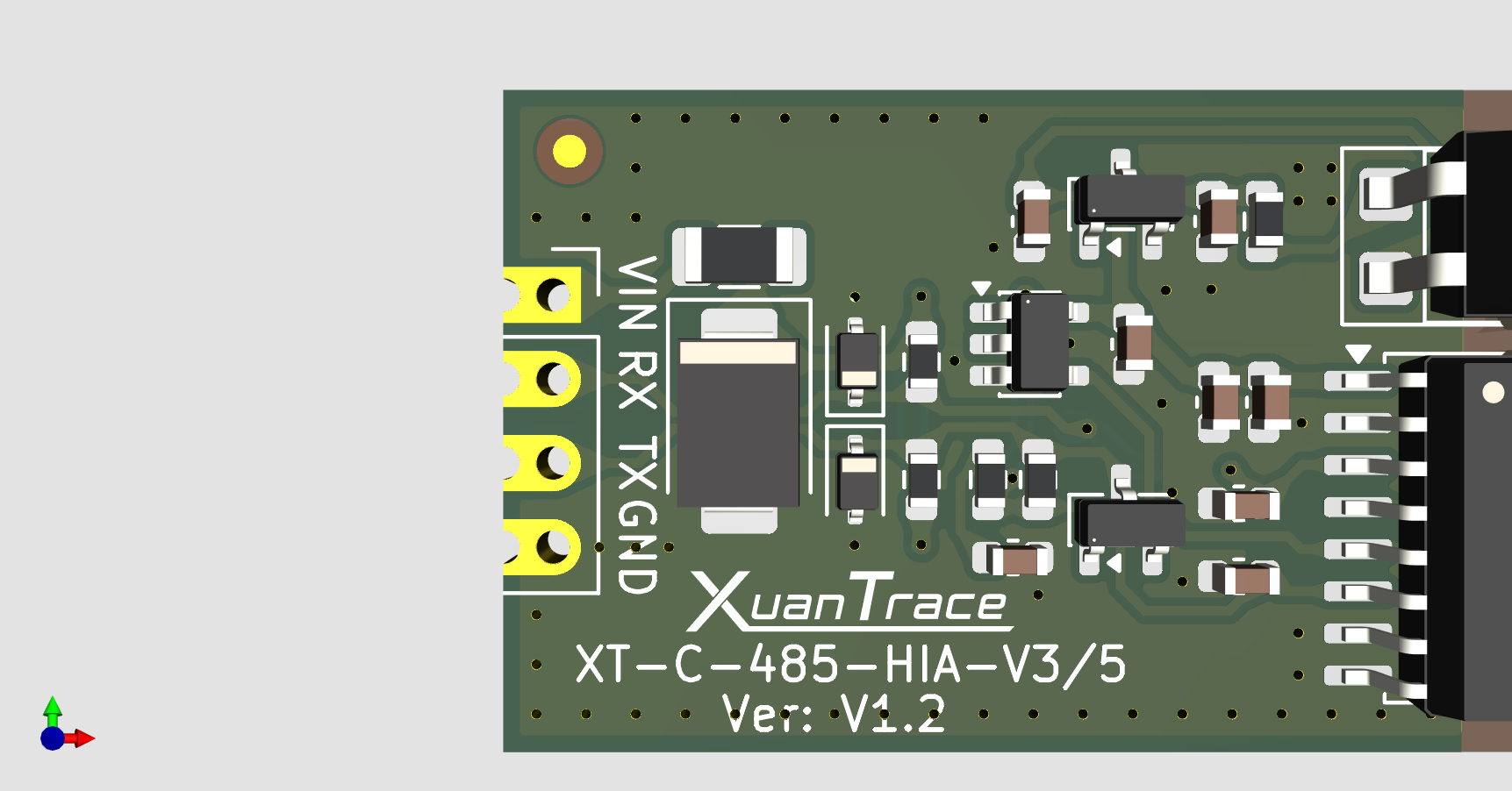
| Name | Flow | Description |
|---|---|---|
VIN | — | Supply 3.0 – 5.5 V (3.3 V / 5 V typical) |
RX | Module → MCU | Bus data received by the module goes to the MCU; connect to the MCU's RX |
TX | MCU → Module | Data the MCU wants to send goes into the module; connect to the MCU's TX |
GND | — | Logic-side ground, common with the MCU |
Straight-through to the MCU — no crossover: TX to the MCU's TX, RX to the MCU's RX. TX is shaped by a Schmitt trigger and drives the transceiver's RE / DE directly; half-duplex direction switching is automatic, so the software never handles direction.
Bus Side (5.08 mm)
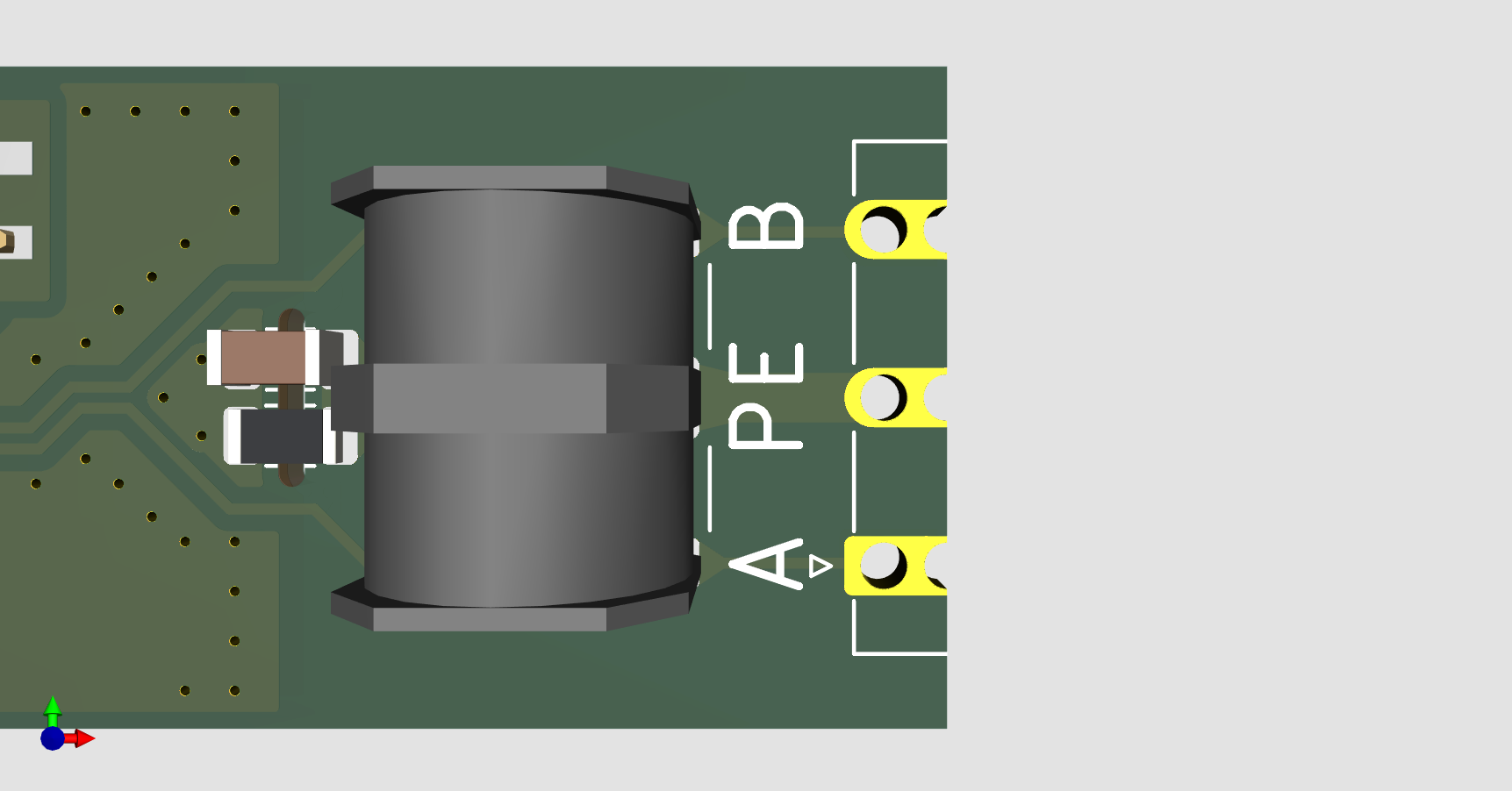
| Name | Flow | Description |
|---|---|---|
B | Bidirectional | RS-485 B (inverting) |
PE | — | Protective earth — must be terminated to earth nearby (the discharge path of the gas discharge tube) |
A | Bidirectional | RS-485 A (non-inverting) |
Wiring Notes
PEmust be terminated to earth nearby: the gas discharge tube usesPEas its discharge path; withPEfloating, surge protection is noticeably weaker.- Never short the isolated-side
PEto the logic-sideGND: once they share ground, the isolation is gone. - Termination: close the on-board jumper for 120 Ω only at the two physical ends of the bus; leave intermediate nodes open.
- Biasing: the module provides A pull-up / B pull-down bias; when you build a multi-node network, work out the parallel bias of the whole bus.
Dimensions
Outline 90 × 20 mm, board thickness 1.6 mm.
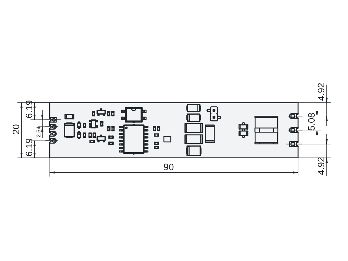
Recommended Pad Dimensions
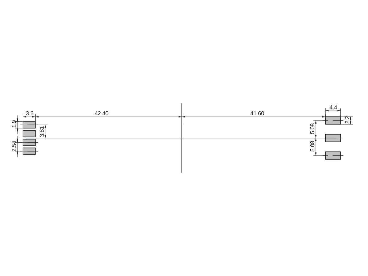
Recommended pads: logic side 3.6 × 1.9 mm (pitch 2.54 mm), bus side 4.4 × 2.2 mm (pitch 5.08 mm); the remaining locating dimensions are in the drawing above.
Electrical parameters are in Specifications; the full parameter table is on the product page.